Home › Unlabelled ›
Full Adder Circuit Diagram : Adder Circuit Explanation with Circuit Diagram : Full adder circuits can be divided into two groups on the basis of output.
Full Adder Circuit Diagram : Adder Circuit Explanation with Circuit Diagram : Full adder circuits can be divided into two groups on the basis of output.. Full adder definition, block diagram, truth table, circuit diagram, logic diagram, boolean expression and equation are discussed. The first half adder circuit will be used to add a and b to produce a partial sum. You can edit this template and create your own diagram. As with the full adder, full subtractors can be strung together (the borrow output from one digit connected to the borrow input on the next) to build a circuit to subtract arbitrarily long binary numbers. Consider adding two binary numbers together:
Thus, this is all about the adder circuit explanation in brief with circuit diagram, which includes a half adder. A full adder circuit is central to most digital circuits that perform addition or subtraction. In the block diagram, a0 and b0 represent the lsb of the four bit words a and b. Here, by using complicated hardware, the propagation delay can be minimized. The truth table and corresponding karnaugh maps for it.
Full Adder : Circuit Diagram, Truth Table, Equations ... from www.watelectronics.com Adder is a combinational circuit that performs the addition operation of 3 input bits. Adders are classified into two types: Cddx circuit netlist png image svg image. The first half adder circuit will be used to add a and b to produce a partial sum. Some designs of the full adder circuit based on transmission gates are shown in figure 3. A, b and cin, which add three input binary digits and generate two binary outputs i.e. Full adder logic gate circuit diagram template. Full adder is a combinational logic circuit used for the purpose of adding two single bit numbers with a carry.
Can someone draw a circuit diagram of 4 bit carry look ahead adder.
Full adder circuits can be divided into two groups on the basis of output. Adder is a combinational circuit that performs the addition operation of 3 input bits. We should also take a glance on the truth tables of these adders. We see that the bit in the two's column is generated when the addition carried over. And an output circuit section. Here you can design and simulate your own electronic circuits. Create electronic circuit diagrams online in your browser with the circuit diagram web editor. The adder adds the two inputs a and b in parallel producing the sum s. Creately diagrams can be exported and added to word, ppt (powerpoint), excel, visio or any other document. Adders are classified into two types: In fact a single circuit is generally used for. This full adder logic circuit is used to add three binary numbers, namely a, b and c, and two o/ps sum and carry. From wikimedia commons, the free media repository.
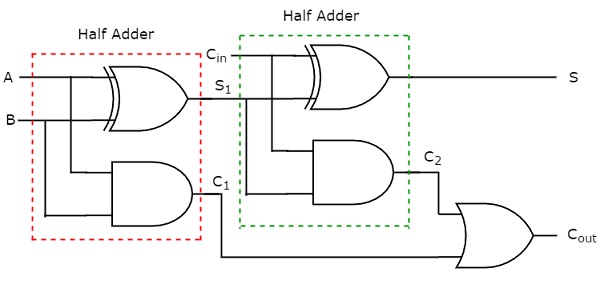
The first half adder circuit will be used to add a and b to produce a partial sum. Jump to navigation jump to search. The truth table and corresponding karnaugh maps for it. The first half adder circuit is on the left side, we give two single bit binary inputs a and b. Full adder s have been already explained in a previous article and in this topic i am giving nand gates or nor gates can be used for realizing the half adder in universal logic and the relevant circuit diagrams are shown in the figure below.
Proposed full adder schematic diagram | Download ... from www.researchgate.net This is the full adder circuit diagram with the detailed explanation of its working principles. The full adder (fa) circuit has three inputs: Figure 2 is a schematic diagram showing a second embodiment of a cmos full adder circuit, according to the present invention; Some designs of the full adder circuit based on transmission gates are shown in figure 3. It can be used in many applications like, encoder, decoder, bcd system, binary calculation two input xor gate, two input and gate, two input or gate forms the full adder logic circuit, input & output of this logic. The first half adder circuit is on the left side, we give two single bit binary inputs a and b. Consider adding two binary numbers together: And an output circuit section.
The first half adder circuit will be used to add a and b to produce a partial sum.
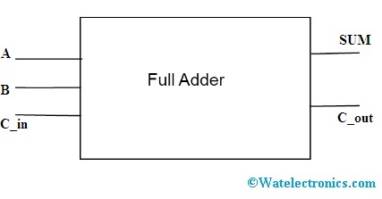
A full adder is the digital circuit which implements addition operation on three binary digits. The electronic circuit simulator helps you to design the you can easily design the full adder circuit by practicing the exercises given below. Hence, there will be four addition combinations these two binary digits and those. The two output variables are expressed by sum(s) and carry (c out ) 4. 1 shows the essential block diagram of full adder cell. Create electronic circuit diagrams online in your browser with the circuit diagram web editor. The full adder circuit diagram add three binary bits and gives result as sum, carry out. Full adder circuit construction is shown in the above block diagram, where two half adder circuits added together with a or gate. Cddx circuit netlist png image svg image. Adder circuits are of two types: The truth table and corresponding karnaugh maps for it. A binary bit is either 0 or 1. A full adder circuit is central to most digital circuits that perform addition or subtraction.
Notice that subtractors are almost the same as adders. Adders are classified into two types: Full adder definition, block diagram, truth table, circuit diagram, logic diagram, boolean expression and equation are discussed. This full adder logic circuit is used to add three binary numbers, namely a, b and c, and two o/ps sum and carry. This is the full adder circuit diagram with the detailed explanation of its working principles.
QCOM - Page 2 - FREE TUTORIALS from www.tutorialspoint.com We see that the bit in the two's column is generated when the addition carried over. As with the full adder, full subtractors can be strung together (the borrow output from one digit connected to the borrow input on the next) to build a circuit to subtract arbitrarily long binary numbers. A, b and cin, which add three input binary digits and generate two binary outputs i.e. It can be used in many applications like, encoder, decoder, bcd system, binary calculation two input xor gate, two input and gate, two input or gate forms the full adder logic circuit, input & output of this logic. Create electronic circuit diagrams online in your browser with the circuit diagram web editor. A circuit diagram of half adder and full adder is shown in the figure below, figure 1: Thus, a full adder circuit can be implemented with the help of two half adder circuits. Full adder is developed to overcome the drawback of half adder circuit.
We should also take a glance on the truth tables of these adders.
The full adder circuit diagram is shown below Hence, there will be four addition combinations these two binary digits and those. Jump to navigation jump to search. Full adder circuit construction is shown in the above block diagram, where two half adder circuits added together with a or gate. Thus, a full adder circuit can be implemented with the help of two half adder circuits. This full adder logic circuit can be implemented with two half adder circuits. Full adder is a combinational logic circuit used for the purpose of adding two single bit numbers with a carry. A binary bit is either 0 or 1. Some designs of the full adder circuit based on transmission gates are shown in figure 3. A full adder is the digital circuit which implements addition operation on three binary digits. Full adder s have been already explained in a previous article and in this topic i am giving nand gates or nor gates can be used for realizing the half adder in universal logic and the relevant circuit diagrams are shown in the figure below. The first half adder circuit is on the left side, we give two single bit binary inputs a and b. Figure 2 is a schematic diagram showing a second embodiment of a cmos full adder circuit, according to the present invention;